Air-Bridge Optoelectronic Devices via Direct Cold Weld Bonding
TECHNOLOGY NUMBER: 2020-159

OVERVIEW
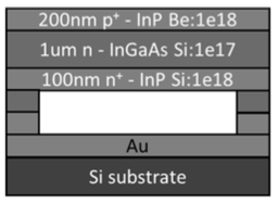
A method of fabricating thin film devices via direct cold welding that creates an air bridge- Air bridge resides between a semiconductor thin film device and a reflector
- Leads to a > 99% reflectance in the spectra range of interests
BACKGROUND
Light management is critical to maximize open circuit voltage for many optoelectronic devices such as photovoltaic (PV) cells, thermophotovoltaic (TPV) cells, photodetectors (PD), light-emitting diodes (LEDs), etc. Thin film devices with high quality back reflectors often show superior properties over conventional bulk substrate devices in this setting. For example, high reflectance mirror targeting at the bandgap energy of a PV cell enhances the photon-recycling effect, leading to a substantial increase in the open circuit voltage. A high-quality mirror that improves the sub-bandgap reflectance in a thin film TPV cell may lead to significant improvement in its overall power conversion efficiency. However, current approaches for optimizing light management such as the use of metal mirrors, photonic crystals, and metamaterials, are usually limited in their effectiveness since they commonly create less than 95% of reflectance in the spectra range of interests. So, a need exists to improve the sub-bandgap reflectance in a thin film optoelectronic device and increase the overall power conversion efficiency.
INNOVATION
Researchers have created a method of fabricating thin film devices via direct cold welding that creates an air bridge between a semiconductor thin film device and a reflector. In this approach, the thin film active layer is grown on a parent substrate that is later removed via epitaxial lift off or by substrate etching. The process can therefore utilize an air gap or another low index dielectric material to achieve the desired configuration. The refractive indices contrast between the semiconductor thin film and the air-bridge maximize the reflectance at their interface. The resulting high dielectric mismatch leads to a > 99% reflectance in the spectra range of interests. The potential applications for this advancement are wide and include thin film photovoltaic cells, solar panels, and thermophotovoltaic cells.
PATENT APPLICATION
Number: US20210328087