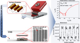
Rubbing-Induced Site-Selective Growth (RISS) of Device Patterns
TECHNOLOGY NUMBER: 2018-464

OVERVIEW
An approach capable of directly generating device patterns of nanomaterials- Does not require resist-based lithography and etching processes
- Produces Molybdenum disulfide lines for transistors and memristors
BACKGROUND
The process for producing semiconductor integrated circuits and microchips is complex and requires incredible precision and uniformity to ensure high yields. Sensitivity to potential contaminants dictates that they be produced in clean room settings. Emerging low-dimensional nanomaterials, such as 2D materials, have provided new opportunities in making electronic and optoelectronic devices. To manufacture commercially viable devices/systems based on such nanomaterials, conventional resist-based lithography and plasma-based etching processes need to be performed to pattern the raw material films into orderly arranged device patterns. Such conventional patterning processes can inevitably introduce serious contamination and damage to the patterned materials and therefore result in inconsistent electronic properties. So, a need exists for a process for producing circuits and microchips while minimizing damage to the atomically-thin structures of nanomaterials.
INNOVATION
Researchers have invented an approach capable of directly generating device patterns of nanomaterials without additional resist-based lithography and etching processes. The methodology consists of two steps, the first of which involves a damage-free rubbing process for generating triboelectric charge patterns on a dielectric surface, while the second consists of site-selective chemical vapor deposition of target nanomaterials within rubbing-induced charge patterns. This rubbing-induced site-selective growth (RISS) method demonstrates production of Molybdenum disulfide (MoS2) lines over large areas as well as arrays of field-effect transistors and memristors. This new method for applying 2D materials to electronic substrates that does not rely on the photo-resist method, and thus mitigates many of the current limitations created by the use of the materials in electronic applications. Additionally, the reliance on simple mechanical rubbing and chemical vapor deposition indicates that the technology is likely to be readily scalable to industrial production.
PATENT APPLICATION
Number:US20200176250
-
expand_more mode_edit Inventor (2)Byunghoon RyuXiaogan Liang
-
expand_more library_books References (1)
- Ryu B, Li D, Park C, Rokni H, Lu W, and Liang X. , Rubbing-induced site-selective growth of MoS2 device patterns. ACS Appl. Mater. Interfaces. November 28, 2018. https://doi.org/10.1021/acsami.8b15108
-
expand_more cloud_download Supporting documents (1)Product brochureRubbing-Induced Site-Selective Growth (RISS) of Device Patterns.pdf