Self-Erasable and Rewritable Optoexcitonic Platform for Anti-Tamper Hardware
TECHNOLOGY NUMBER: 2021-082

OVERVIEW
An optical scratch pad to detect and mitigate ICs- Provides a memory which is self-destructible
- Responds to light or temperature changes
BACKGROUND
Counterfeit integrated circuits (IC) are a concern in the electronics industry because their inferior quality, reliability, and performance can cause equipment failure. System malfunctions due to IC can lead to safety hazards across important computer platforms utilized in the aerospace, defense, and medical equipment industries. Manufacturer attempts to prevent counterfeited technologies are multifactorial and include strengthening intellectual property laws, optimizing supply chain traceability, and utilizing technical approaches that set standards for device testing and certification. Existing technological approaches involve the imbedding of security features within the IC devices themselves. Examples of these features include tamper-evident packaging, holographic labels, and unique identification codes. Additionally, testing and verification methods may include X-ray analysis, infrared imaging, and electrical testing. Still, a need exists for improved ways to validate an IC and determine whether it has been counterfeited, ensuring the safety and reliability of electronic devices.
INNOVATION
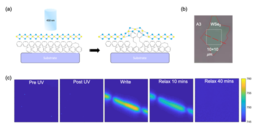
Researchers have invented an approach that utilizes nanoscale strain engineering to create a self-erasable and rewritable platform for anti-tamper hardware. The inventors created a material consisting of a monolayer of WSe2 (a transition metal dichalcogenide) layered on top of layers of azobenzene (A3) molecules. The reversible structural change between trans and cis isomers inazobenzene (A3) molecules is used to strain the overlying tungsten diselenide (WSe2) monolayer, thereby affecting its optical bandgap. Using such hybrid material combinations, the innovators generated large (>1%) local strain that resulted in a dramatic shift (> 11 nm) in photoluminescence wavelength. The strain in layered A3 films can be rapidly relaxed under exposure to visible light or can be retained up to seven days under dark conditions.
By utilizing hyperspectral imaging, the technology demonstrates a self-erasable and rewritable optoexcitonic platform that responds to environmental changes, such as those related to light or temperature, to detect tampering of the hardware system. In addition, the results open avenues for varied applications in information storage, time sensitive self-destructive memories to light detection. In short, this technology is a device that responds to the environmental conditions of light and heat in the form of photoluminescence, with the degree of photoluminescing being able to be controlled by layering of A3 molecules and with the technology being able to self-erase due to relaxation or white light exposure.
-
expand_more mode_edit Inventor (4)Che-Hsuan ChengDa Seul YangJinsang KimParag Deotare
-
expand_more library_books References (1)
- Cheng C, Yang D, Kim J, and Deotare P. , Self-Erasable and Rewritable Optoexcitonic Platform for Antitamper Hardware, Advanced Optical Materials 8(21)10.1002/adom.202001287
-
expand_more cloud_download Supporting documents (1)Product brochureSelf-Erasable and Rewritable Optoexcitonic Platform for Anti-Tamper Hardware.pdf