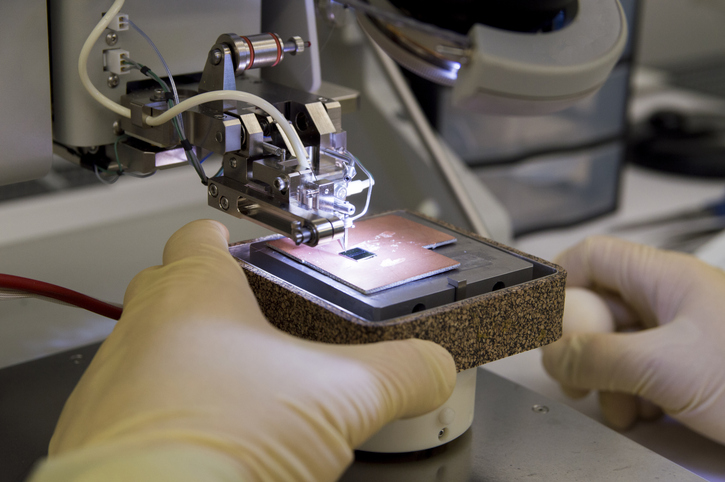
Wafer-Level Fabrication of MEMS and Solid-State Devices
TECHNOLOGY NUMBER: 4440

OVERVIEW
Integration of bulk piezoelectric materials in MEMS with enhanced performance
- Low-temperature bonding preserves bulk piezoelectric properties efficiently
- MEMS devices, solid state sensors, advanced actuator systems
BACKGROUND
Piezoelectric materials have long been integral to both MEMS and solid-state devices owing to their efficient electromechanical conversion properties. Historically, thin-film piezoelectric layers deposited via methods like sol-gel, sputtering, and direct writing suffer from lower piezoelectric coefficients, limited film thickness, and high processing temperatures, which are incompatible with post-CMOS processes. On the other hand, bulk piezoelectric ceramics possess high piezoelectric coefficients and structural robustness but lack simple integration into microfabrication techniques. Current thin-film fabrication methods often result in films with significant cracks and reduced effectiveness, creating a pressing need for a reliable, low-temperature, and scalable method to integrate bulk piezoelectric materials into traditional silicon processes for improved MEMS and other applications.
INNOVATION
Researchers at the University of Michigan have developed a novel batch-mode fabrication technology that enables the integration of bulk piezoelectric materials into MEMS devices while retaining their high electromechanical coupling coefficients. The process involves low-temperature, solder and Parylene bonding of PZT wafers or dies on silicon wafers, followed by lapping to achieve the desired film thickness. This approach mitigates common issues like high processing temperatures and stress-induced cracking, and it preserves the bulk piezoelectric properties. The technology is applicable to a variety of piezoelectric materials, such as PZN-PT and PMN-PT, and it supports fabrication of devices in different sizes and shapes. Potential real-world applications include advanced MEMS sensors, solid-state actuators, and low-power consumption devices in smart materials systems.
ADDITIONAL INFORMATION
REFERENCES:
E. E. Aktakka, H. Kim and K. Najafi, "Wafer level fabrication of high performance MEMS using bonded and thinned bulk piezoelectric substrates," TRANSDUCERS 2009 - 2009 International Solid-State Sensors, Actuators and Microsystems Conference, Denver, CO, USA, 2009, pp. 849-852, doi: 10.1109/SENSOR.2009.5285795
INTELLECTUAL PROPERTY:
US8209857 "Method of making a thin film device"